

autor:
Badania - Fizyka powierzchni

Determination of Strain and Stress in Thin Films Using Curvature Measerments
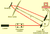
ExperimentSi (001) wafer (5", 180 µm thick) with 1000 Å film of deposited gold was cut along (100) direction. A radius of curvature of each sample was measured in (010) direction with two different setups (fig. 1).
 a | 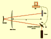 b |
First one (fig. 1a) consists of focusing lenses, manually positioned mirror, main lens, video camera and PC. As a source of light we used a laser diode. The laser beam reflects from the mirror and goes through the main lens. Reflected from the surface of a sample goes again through the main lens and finally hits the CCD camera. The image from the camera is forwarded through a video capture card to the computer. A program processes the image and determines a position of a spot of the laser beam on the CCD. The lenses focus a laser beam on the CCD in order to obtain the highest accuracy of the spot position. The second setup (fig. 1b) [1, 2] uses a position sensitive detector (PSD) instead of CCD, and a computer positioned mirror.
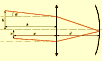
Fig. 2: Optic system of both setups.
Both setups are based on the optic system shown in fig. 2. One can deduce a relation for all parameters of the optic system using basic laws of optics. When a and b are equal to a focal length of lens f we get the simple relation:
 (1)
(1)Thus the displacement of the spot when the angle q is changing determines a radius of curvature R of investigated surface. For flat surface focal point is in the same plane as a mirror and a movement of the spot is not observed. Concave and convex surfaces shift this point from the focal plane and move the spot on the detector. A type of bending (a sign of a radius of curvature) is determined by the direction of movement of a spot on the detector.
The radius of curvature corresponds to the biaxial stress s in agreement with Stoney's formula:
 (2)
(2)
Fig. 3: Positions of the spot on CCD and PSD for sample 1.
Positions of the spot on CCD and PSD for sample 1 are shown in fig. 3. We calculated average displacements using a linear fit. The radius of curvature and stress for each sample were calculated from equations 1, 2 and are shown in fig. 4. Results from both setups are in a very good agreement. One should take into account that a measured radius of curvature depends very strongly on area of a scan. A strain of the wafer is not homogeneous. Even sign of radius of curvature changes for investigated wafer. Stress in the samples changes from -0.17 Gpa to 0.3 GPa. Analysis of plot from fig. 3 gives also information about irregularity of a bend of the sample. Inhomogeneous strain of the wafer may be caused by structure imperfections in substrate as well as in the deposited layer.
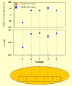
Fig. 4: Radiuses of curvature and corresponding stresses of the samples obtained with two setups. At the bottom: the placement of the samples in a silicon wafer.
First setup (fig. 1a) provides possibility of biaxial measuring of the displacement of a spot. It enables more detailed analysis of the investigated surface. On the other hand it requires more time to process or to store an image from CCD. A signal form PSD corresponds to a position of the spot and it is available at once. This feature allows increase a number of measurements in a time unit.
AcknowledgementsWe would like to thank O. Thomas, P. Gergaud and Ola from MATOP [2] for the access to the setup 2.
References
[1] S. Labat, Diplome d'Etudes Approfondies, Université Aix-Marseille III, 1994.
[2] MATOP, URA CNRS 1530, Faculté de St Jérôme F-13397 Marseille Cedex 20, France.